
Typical Applications
- Semiconductor wafers
- Precision semiconductor manufacturing
- Protected storage and transfer
Precision-engineered packaging bags for semiconductor wafers, designed to support contamination control and electrostatic protection.
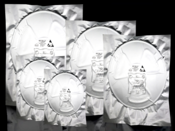
For dimensions, printing, material structures or application-specific requirements, contact us for a tailored recommendation.
Request a Quote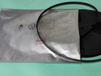
Secure packaging solutions for electronic reels, supporting moisture resistance and mechanical protection during transit and storage.
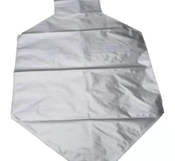
Custom protective packaging can be tailored to specific product dimensions and specialized packaging needs, including large-capacity and long-form bags.
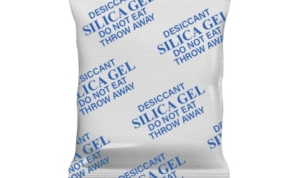
Desiccant actively absorbs residual moisture inside packaging to help maintain a low-humidity environment. Available types include silica gel and montmorillonite clay.